

Device Lab (Goa)
- Facilities
- Device Lab (Goa)
The BITS BioCyTiH Device Lab is a specialized facility dedicated to the prototyping, testing, and validation of hardware and sensory systems within the Bio-Cyber-Physical Systems (Bio-CPS) domain. Its core purpose is to provide innovators with precision engineering tools and advanced fabrication equipment—such as Lithography, PCB prototyping stations, and high-end signal analyzers—to transition from theoretical designs to functional medical and environmental devices. By integrating hardware development with digital intelligence, the lab facilitates the creation of “smart” diagnostic tools, wearable health monitors, and automated biological sensors, ensuring these devices meet the rigorous technical and safety standards required for clinical and industrial application.
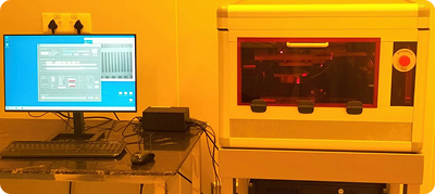
Maskless Lithography
Key Features:
- Maskless Patterning
- Substrate Versatility
- Multi-layer lithography with high alignment accuracy (~±0.5 µm or better).
- Pattern Complexity
- Software Integration such as GDSII, DXF, Gerber, STL
- Non-Vacuum Process
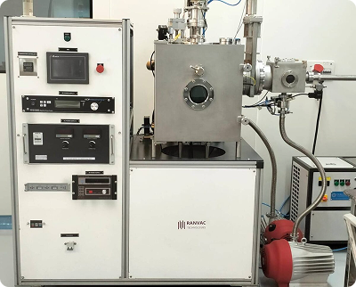
RF-DC Sputtering
Key Features:
- Dual Power Modes (RF + DC)
- Uniformity & Film Quality
- Deposition Rate vs Material Trade-off
- Vacuum System / Pressure Control
- Substrate Heating / Biasing
- Multi-Gun & Reactive Sputtering Options
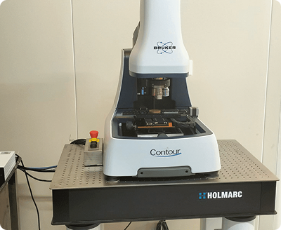
3D Optical Surface Profiler
Key Features:
- Non-Contact Measurement
- High Vertical & Lateral Resolution
- 3D Surface Topography
- Wide Measurement Range
- Fast, Automated Scanning
- Versatility in Applications
- Advanced Software Integration
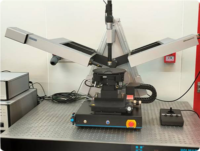
Spectroscopic Ellipsometer
Key Features:
- Non-Destructive & Non-Contact.
- Thin Film Thickness Measurement
- Optical Constants (n & k)
- Multi-Layer Capability
- Spectroscopic Analysis
- Polarization-Based Technique
- Automation & Modelling Software
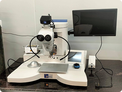
Wire Bounder
Key Features:
- Ball bonding & wedge bonding
- Wire / Ribbon Types & Sizes of 17 µm to 75 µm (Au, Al).
- Motorised Z- and Y-axes for the bond tool. X-axis usually manual.
- Automatic bond height adjustment via a Z-axis sensor (touch-down sensing).
- Loop Profile Programming
- Store many bonding parameter sets/recipes (roughly 100).
- 6.5-inch TFT touch panel for controlling parameters, selecting mode, etc.
- Heated Work Stage
- Wire Clamp & Spool Motorization
- Built-in stereo microscope (zoom) and options like laser spotlight / target system to assist alignment.
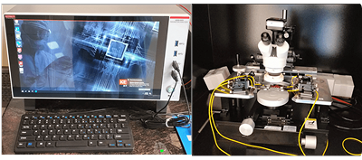
Semiconductor Parameter Analyzer With Probe Station
Key Features:
- Electrical Measurement Capabilities
- Probe Station Integration
- Device Versatility
- Data Analysis & Modelling
- User Interface & Automation
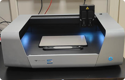
Voltera NOVA PCB printer
Key Features:
- High-resolution direct ink writing with minimum trace width down to 100 μm
- Closed-loop pressure control for precise material dispensing.
- Automated height mapping for consistent print quality across uneven substrates.
- User-friendly browser-based interface with Wi-Fi/Ethernet connectivity and Gerber file format compatibility