DEVICE LAB
It has cutting-edge technologies that are used to design, prototype and test electronic devices.
Location: Goa
Semiconductor Parameter Analyzer With Probe Station
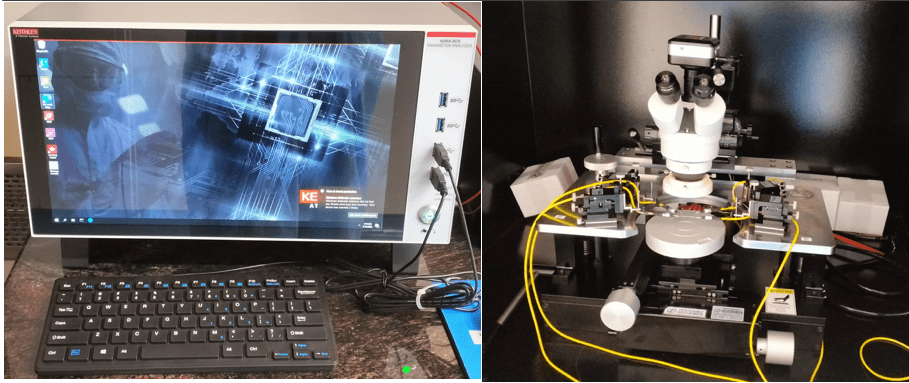
Key Features:
- Electrical Measurement Capabilities: I–V (Current–Voltage) and C–V (Capacitance–Voltage) characterization of semiconductor devices. Multi-SMU support.
- Probe Station Integration: Precise micro-positioners with sharp probes to contact device pads. Works for wafer-level and chip-level testing.
- Device Versatility: MOSFET, JFET, Diode, LED, Biosensor, photodetector, solar cell, MEMS, and nanoscale device testing.
- Data Analysis & Modelling: : Built-in software for parameter extraction (threshold voltage, mobility subthreshold slope, etc.). Automated sweep and curve fitting.
- User Interface & Automation: PC-based control with graphical software. Low-noise triaxial cabling for ultra-low current measurements.
3D Optical Surface Profiler
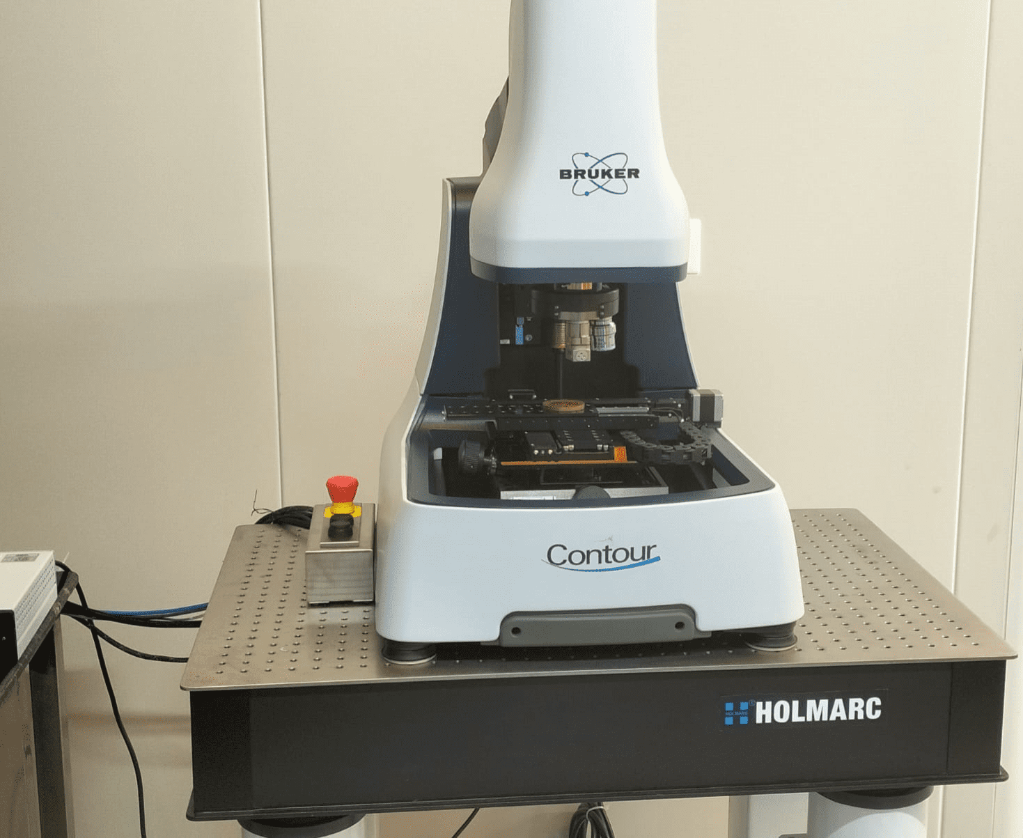
Key Features:
- Non-Contact Measurement: Uses white light interferometry or confocal optics. No damage or contamination of delicate samples. Can measure in ambient air (no vacuum required).
- High Vertical & Lateral Resolution: Vertical resolution of nanometre scale. Lateral resolution depends on objective lens, typically < 1 µm
3D Surface Topography: Generates 3D surface maps with accurate height information. Suitable for step height, roughness, texture, and microstructure measurement. - Wide Measurement Range: Can measure surface heights from a few nanometres to several millimetres. Works on smooth, rough, reflective, and transparent surfaces.
- Fast, Automated Scanning: Rapid, non-destructive measurements. Motorized stages for large area stitching and mapping.
- Versatility in Applications: Thin-film thickness measurement. MEMS & microelectronics inspection. Surface roughness (Ra, Rq, Rz, etc.) analysis. Step height and pattern structure profiling.
- Advanced Software Integration: Automated data analysis, filtering, and report generation. Supports 2D/3D visualization, contour maps, and statistical analysis.
Ellipsometer
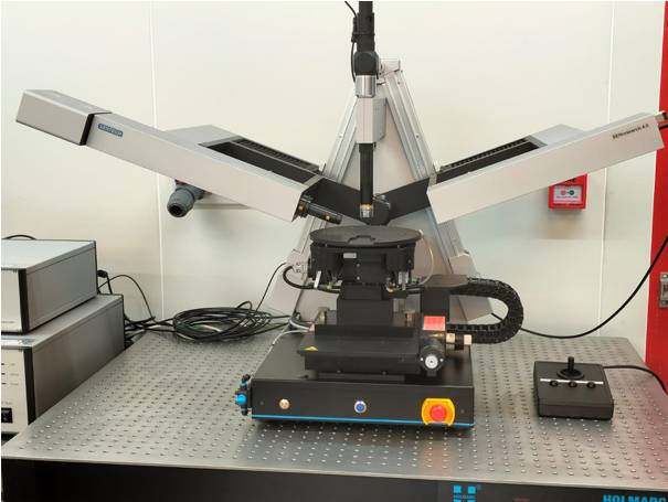
Key Features:
- Non-Destructive & Non-Contact: Measures films and surfaces without damaging or altering the sample.
- Optical Constants (n & k): Determines refractive index (n) and extinction coefficient (k) of materials.
- Multi-Layer Capability: Can characterize single layers and complex multi-layer stacks (dielectrics, metals, semiconductors, polymers).
- Spectroscopic Analysis: Spectroscopic ellipsometers measure across a broad wavelength range (UV–Vis–NIR), providing dispersion data.
- Polarization-Based Technique: Works by analyzing changes in the polarization state of light after reflection/transmission.
- Automation & Modelling Software: Advanced software for data fitting, optical modelling, and material parameter extraction. Automated measurement routines for high-throughput labs.
Wire Bounder
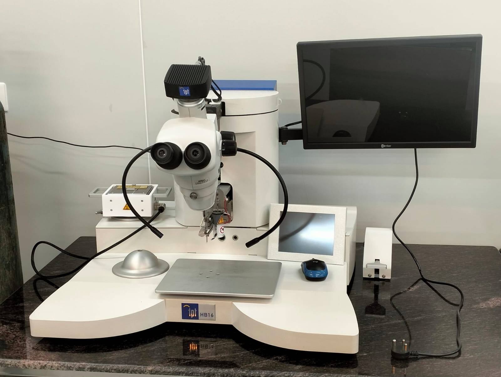
Key Features:
- Bonding Modes: Ball bonding, wedge bonding
- Wire / Ribbon Types & Sizes: Wire: 17 µm to 75 µm (Au, Al).
- Axes / Movement: Motorised Z- and Y-axes for the bond tool. X-axis usually manual.
- Touch / Height Control: Automatic bond height adjustment via a Z-axis sensor (touch-down sensing).
- Loop Profile Programming: Able to program loop profiles (up to ~10 steps) so loops are repeatable and adjustable.
- Recipe / Parameter Storage: Can store many bonding parameter sets/recipies (roughly 100).
- User Interface: 6.5-inch TFT touch panel for controlling parameters, selecting mode, etc.
- Heated Work Stage: Heated work stage available (often up to ~250 °C) for temperature-sensitive bonding. Vacuum or mechanical clamping options.
- Wire Clamp & Spool Motorization: Motorized wire clamp (for tail-length control) and wire spool motorization for feed consistency.
- Microscope / Alignment: Built-in stereo microscope (zoom) and options like laser spotlight / target system to assist alignment.
RF-DC Sputtering
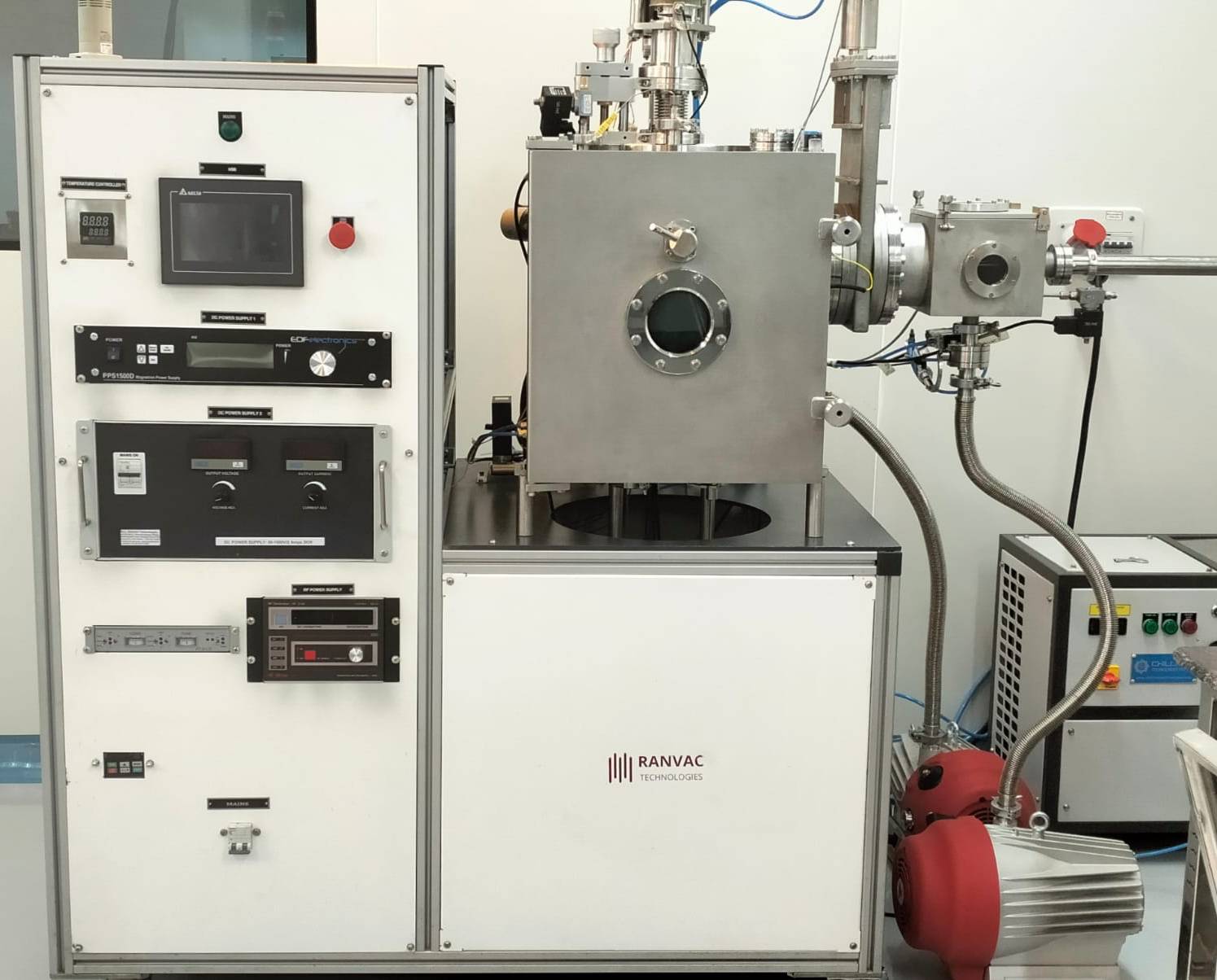
Key Features:
- Dual Power Modes (RF + DC): Ability to switch or combine DC and RF power sources depending on target material. DC mode is good for conductive targets (metals etc.), RF mode allows deposition of insulating/dielectric materials without charge build-up.
- Plasma Control / Match Network: RF power systems need impedance-matching networks and blocking capacitors; they maintain and sustain plasma especially for insulating targets.
- Uniformity & Film Quality: Ability to deposit uniform films, good step coverage, density, smooth morphology. RF helps with better uniform films for dielectrics; DC often gives higher deposition rates for metals.
- Deposition Rate vs Material Trade-off: DC mode generally yields higher deposition rate for conductive materials; RF mode is slower (due to lower ion current densities etc.), but possibly better film properties (less defects, better uniformity)
- Vacuum System / Pressure Control: Needs good vacuum (low base pressure), control of inert gas (Ar) flow, possibly reactive gases. Lower pressure for better film purity. Many systems have load-lock, or dual chambers and good pumping to maintain clean environment.
- Substrate Heating / Biasing: Chambers allow substrate heating affect film crystallinity, stress, adhesion. Thermal control beneficial.
- Multi-Gun & Reactive Sputtering Options: Having multiple sputter guns so that co-sputtering or sequential deposition without breaking vacuum is possible; also reactive sputtering (with gases like O₂, N₂) to deposit oxides, nitrides etc.
Maskless Lithography
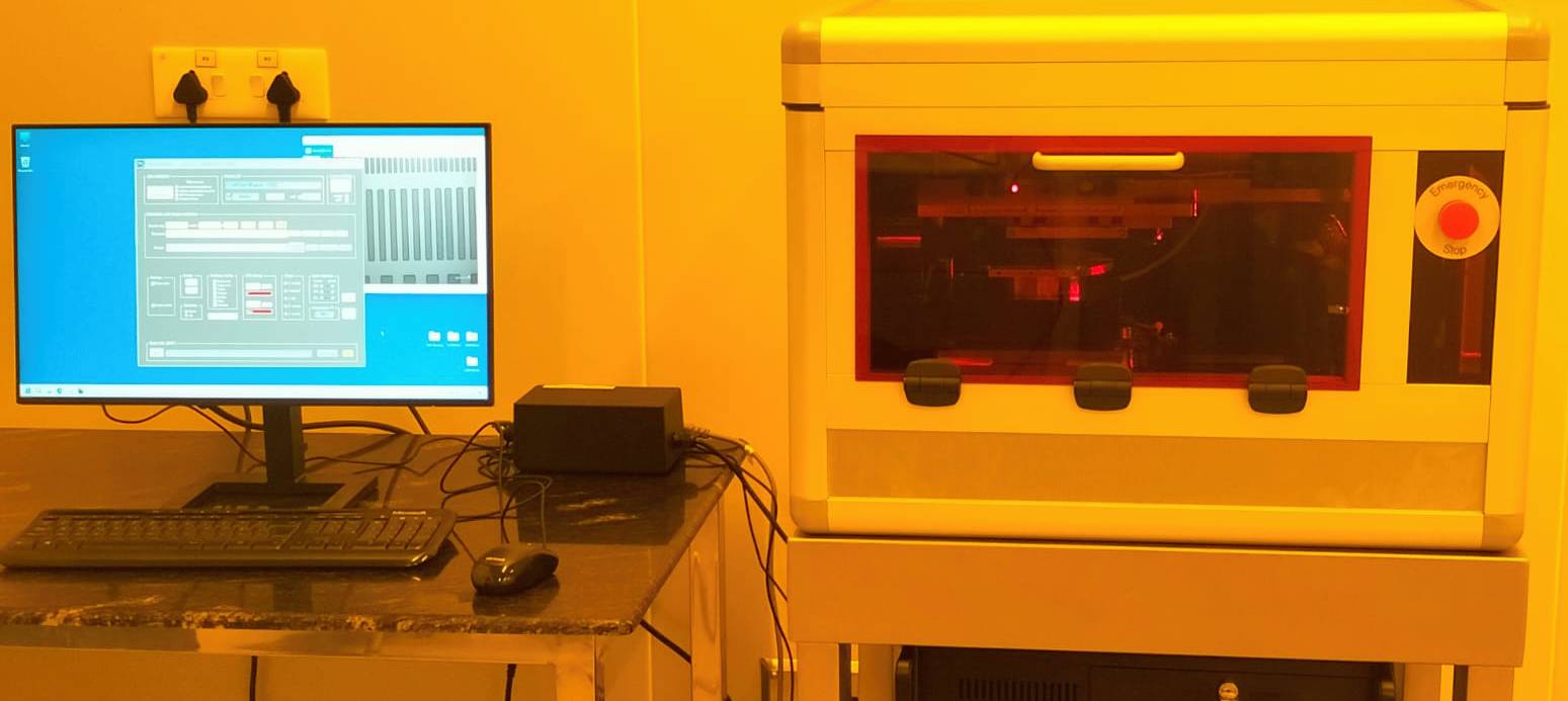
Key Features:
- Maskless Patterning: Eliminates the need for costly chrome masks. Patterns are directly written from a digital design file.
- High Flexibility: Easy design changes (just update the file). Ideal for R&D, prototyping, and low-volume fabrication.
- Resolution & Feature Size: Typical resolution: ~0.5 µm to few µm.
- Substrate Versatility: Works on wafers, glass, polymers, MEMS substrates, flexible materials. Compatible with various positive and negative photoresists.
- Automation & Alignment: Computer-controlled stage with automatic alignment marks recognition. Can do multi-layer lithography with high alignment accuracy (~±0.5 µm or better).
- Pattern Complexity: Can generate arbitrary complex geometries, grayscale lithography, 3D microstructures, and micro-optical elements.
- Software Integration: Supports direct import of GDSII, DXF, Gerber, STL files. Real-time pattern editing and parameter control.
- Non-Vacuum Process: Operates under ambient or cleanroom conditions (no vacuum chamber needed).
- Applications: Semiconductor prototyping, MEMS, photonic devices, diffractive optics. Microfluidics, biochips, polymer devices. R&D environments where fast turnaround is critical.
